Seeing in the Dark
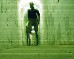
Thermal imaging cameras now used to protect assets and prevent vandalism, terrorism or random acts of violence
- By Dan Ostrower
- Sep 01, 2006
 THE desire to see in complete darkness or through smoke or fog has driven the development and adoption of thermal imaging technology. Specifically in the security and surveillance sector, thermal imaging cameras are an essential part of security programs to protect assets and prevent vandalism, terrorism or random violent attacks.
Specifically in the security and surveillance sector, thermal imaging cameras are an essential part of security programs to protect assets and prevent vandalism, terrorism or random violent attacks.
Thermal imaging is the translation of a scene's heat signature -- the 8 um to 14 um, or long wavelength infrared energy (LWIR), it emits -- into a visible image or data that can be interpreted by a computer. Because the thermal energy of a scene is largely independent of reflected light and because it can travel through many obscurants, thermal imaging is the technology of choice for imaging in the dark or other difficult environmental conditions. There is great demand -- much of it untapped -- for thermal imaging technology in markets such as firefighting, law enforcement, surveillance, homeland security, industrial and consumer applications.
Specifically, in the security and surveillance markets, combining a conventional video camera with a thermal imaging camera is an added advantage of providing good imaging capabilities in bad weather situations when conventional cameras are unable to perform satisfactorily.
Visible light and near-infrared radiation, to which modern day commercial video cameras and their imaging sensors are responsive, have spectral components that lie between 0.4 to 1.1 microns. The wavelengths of the thermal energy of interest lie between 7.5 and 15 microns. The latter therefore go undetected.
"Until recently, the only camera technology that worked satisfactorily at these thermal wavelengths used cameras with cryogenically-cooled imagers and carried a cost of between $5,000 and $50,000," said David Terrett of J.P. Freeman Laboratories. "Their use is therefore limited to military or very sophisticated industrial applications that can afford the high unit cost."
There are several characteristics that have to be fulfilled to make thermal imaging cameras universally deployable.
Low cost and easy to manufacture. The technology must be manufacturable for a low cost even in modest volumes. This is only possible with high yields and liberal use of technology and manufacturing platforms developed for other high-volume, high-tech industries.
Easily scalable. Different applications have varying needs in terms of resolution, sensitivity and other parameters. Any universally deployable technology must be easily scalable, so that product variety can be provided without excessive development time or expense.
Low power. Many thermal imaging cameras must be small, lightweight and portable. Today, the batteries used to power the system limit size and weight reduction. Lower power consumption -- and thus smaller batteries -- are required to make cameras smaller, lighter and more widely usable.
Good image quality. A univerally deployed thermal imaging technology must be capable of producing images of sufficient quality for the applications in which it is used.
Dissecting the Microbolometer
Today the most common form of thermal imaging technology available is the microbolometer sensor. Microbolometers are built using vanadium oxide (VOx) or amorphous silicon (aSi) processes. Typical prices for microbolometer-based cameras range from $8,000 to $20,000, depending on resolution, performance and feature set.
Microbolometer pixels are complex. The pixel is shaped like a table with two legs that separate it from a substrate and read out integrated circuit below. The "table" is made of electrically-conductive material, such as VOx, and forms a complete circuit with the underlying electronics. When incident LWIR energy strikes the table top the electrical resistance of its materials change. More incident radiation causes a greater change in resistance. The change in resistance can be probed by passing a current through the device. Change in temperature can be read out as electronic signals and used to produce an image. A reason the pixel design becomes complex is because the legs must both thermally isolate the pixel (in order to produce response) and conduct electricity (so that response can be probed). It is not straightforward to produce both results with a single design.
A complete microbolometer camera engine includes several elements: optics, the microbolometer sensor, which consists of a sensing pixel array, read-out integrated circuit (ROIC) and vacuum package and back-end electronics.
The microbolometer sensor is manufactured using a micro-electro-mechanical system (MEMS) process, typical in a custom foundry with specialized VOx processing capability.
First, a custom ROIC wafer is manufactured. This includes complicated circuitry required to interpret the thermally-induced resistance variations. Then, pixel arrays are deposited on this wafer. A typical pixel design is fairly complex and can require in more than 30 mask layers when the underlying CMOS layers are included. Once the pixel arrays have been deposited, the wafer is diced into individual die, which are yielded and vacuum packed to create a finished microbolometer sensor. The sensor is then integrated into control and processing electronics. LWIR optics also are affixed. The complete engine is calibrated for performance over ambient temperature and is then ready for sale.
Examination of the microbolometer structure, materials and manufacturing process makes it clear why this technology is unable to fulfill the requirements of universal deployment.
Low cost? No. Microbolometer based cameras average greater than $7,000 per unit. They're manufactured in dedicated custom foundries and their highly complex, multi-mask step designs result in low yields. Also, failed devices include the cost of custom ROIC electronics. Expensive die-level packaging is required because VOx cannot be exposed to the high temperatures required for inexpensive wafer scale packaging.
Easily scalable? No. The cycle time for new microbolometer designs takes several years and costs millions of dollars.
Low power? Limited. The best microbolometer designs consume around 2W for normal operation.
Highly sensitive? Somewhat limited. Large pixel microbolometer designs have demonstrated enough sensitivity for current applications, but future potential may be limited for smaller pixels. The best possible response for VOx microbolometers is a 2.5 percent change per in signal per ?C change in temperature.
The Key to Universal Deployment
A new technology -- with significant changes in underlying design, materials and manufacturing processes -- is required in order to make universal deployment of thermal imaging a reality. That technology is optical thermal imaging. RedShift Systems Corp. has developed the Thermal Light ValveTM ,(TLV) a passive, optical component that makes optical thermal imaging a reality.
Optical thermal imaging does not rely on the change of resistance to measure temperature changes. Instead, optical thermal imaging technologies rely on changes in optical properties when exposed to temperature changes. Instead of electronically read out, such changes are optically read out, using standard digital camera electronics.
Each pixel acts as a passive wavelength converter. Long-wave length infrared radiation from the scene is imaged onto and absorbed by the TLV. This heats up select thermal pixels on the array in direct relation to the thermal signature of the scene. The minimum reflective wavelengths of the pixels shift based upon the thermal energy incident on each. A narrow-band near-infrared light source (NIR) is used to probe the temperature of the pixels across the TLV. This NIR probe signal is reflected off the TLV in varying amounts, depending on the pixel temperature, onto the CMOS imager. The intensity of the light received by the CMOS imager is therefore modulated by the heat signature of the scene.
A thermal image is obtained by measuring the pixel-to-pixel variation in transmission of the NIR probe signal using CMOS imagers.
The TLV tunable optical filter is a Fabry-Perot structure. The structure is amorphous silicon and silicon nitride thin films, which have been used extensively for many years in solar cells and flat-panel displays. These materials are deposited using plasma enhanced, chemical vapor deposition, which is capable of producing uniform, dense materials in high-volume manufacturing environments. The optical filter's minimum reflective wavelength depends on the optical thickness of the cavity -- a product of physical thickness and index of refraction. RedShift achieves tunability by changing the index of refraction. The materials are characterized by a high thermo-optic coefficient, which is defined as the change of index of refraction per degree of temperature change.
The process demonstrates temperature induced changes in optical materials can be used to produce thermal imagery, but it does not address the issue of whether optical thermal imaging is superior to microbolometers in terms of universal deployment.
Several important differences from the microbolometer should be noted:
-
The sensing array is not an electronic device. It is purely a passive layer of optical thin films on glass. This greatly simplifies manufacturing and packaging.
-
The sensing array is manufactured in a standard MEMS foundry, taking advantage of foundry economies of scale to dramatically reduce manufacturing cost over that obtainable with custom fabrication lines.
-
The readout circuit in the optical thermal imaging system is not physically coupled to the sensing array, nor is it a custom design. It consists of off-the-shelf parts, such as laser diodes and CMOS sensors, that can be sourced from high volume optical mouse and consumer camera applications and managed independently from the sensor array. This reduces cost, increases yield and reduces development cycle time.
The differences are critical. The differences in the two processes make optical thermal imaging and TLV cameras far more suitable for universal deployment.
Low cost? Yes. Optical thermal imaging-based cameras will be available for less than $3,000 in low volumes and will rapidly decrease in price over time and volume. The sensing array -- in this case the TLV -- is manufactured in standard semiconductor foundries so no capital investment is required. The TLV requires only four mask steps to produce. This means it is less costly to manufacture and has much higher yields. The ROIC is not yielded with the array. The TLV can be packaged using wafer scale techniques, which significantly reduces the cost of packaging. The ROIC consists entirely of inexpensive off-the-shelf components such as optical mouse lasers and CMOS sensors that are sourced globally and manufactured in extremely high volumes.
Easily scaleable? Yes. With optical thermal imaging, new products will be released on a time scale consistent with consumer products. Since the pixel's thermal isolation does not also have to be electrically conductive, the design is much simpler and can be easily scaled. A change in sensor component is all that is required for new designs.
Low power? Yes. Optical thermal imaging engines will consume well under 1W.The TLV is passive. It consumes no power. The back-end electronics are the same as a digital camera.
Good image quality? High potential. The thermo-optic materials used in Optical Thermal Imaging are very sensitive to temperature changes. The percent change in signal for a one-degree change in temperature is up to 20 times higher in optical thermal imaging than in microbolometers.
To satisfy the strong demand for thermal imaging, a major technological shift is required. Many industry sectors can benefit from a technology that makes thermal imaging cameras affordable, and this will increase safety and security for all involved.
This article originally appeared in the September 2006 issue of Security Products, pgs. 36-38.